

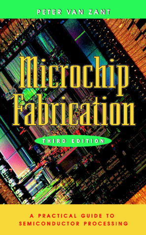
Microchip fabrication
A Practical Guide to Semiconductor Processing
Introduction: Unlocking the Silicon Secret
Introduction: Unlocking the Silicon Secret
Nova: Welcome to 'Silicon Synthesis,' the podcast where we break down the building blocks of our digital world. Today, we are diving deep into the foundational text that many engineers consider the absolute starting point for understanding how a microchip actually gets made: Peter Van Zant's 'Microchip Fabrication.'
Nova: That is precisely the genius of Van Zant's work, Alex. He managed to distill this incredibly complex, multi-billion dollar industry into what many call the 'bible' of basic fabrication. The key takeaway from the research is that this book is famous for being 'low-math' and 'straight-talk.' It covers the journey, from the raw silicon ingot to the finished, packaged device.
Nova: Exactly. It’s the end-to-end narrative. We’re talking about the history, the chemistry, the physics, and the sheer logistical nightmare that is a modern fab. We’ll explore why this foundational knowledge, which Van Zant laid out decades ago, is still critical today, even as we move into the era of chiplets and 3D stacking. Get ready, because we’re going inside the cleanroom.
Key Insight 1: The End-to-End, Math-Free Approach
The Van Zant Method: Demystifying the Fab Process
Nova: Let’s start with the book’s philosophy. Peter Van Zant, who has an extensive background in process engineering, training, and consulting, deliberately structured this book to be accessible. He realized that many technicians and even new engineers were thrown into the cleanroom without understanding the 'why' behind the 'how.'
Nova: He starts right at the beginning: raw materials. We’re talking about taking sand—silicon dioxide—and turning it into a near-perfect single crystal ingot, which is then sliced into wafers. This process, Crystal Growth, is where the purity standard is set. We’re talking about purity levels measured in parts per. If you miss that purity mark here, every subsequent step is doomed.
Nova: He moves into the necessity of the cleanroom, but he frames it contextually. He explains that the entire fabrication process is essentially a highly controlled sequence of adding, removing, and modifying thin films on the wafer surface. The core of the manufacturing, which he dedicates significant space to, is the 'ten-step patterning process.'
Nova: It is the magic, and it’s a cycle that repeats dozens of times. The ten steps generally cover: Surface Preparation, which is crucial for adhesion; Photoresist application; Exposure, using light to transfer the circuit pattern; Developing the exposed resist; Etching to remove material where the resist is gone; Stripping the remaining resist; and then Doping or Deposition to change the electrical properties or add a new layer. It’s a loop of creation and refinement.
Nova: Precisely. And Van Zant emphasizes that the evolution of this process is what drove the industry forward. For instance, the shift from older methods to Jean Hoerni’s planar process, which allowed for easier mass production of integrated circuits, is a historical milestone he covers, showing how process innovation is as important as device innovation.
Nova: Because a perfect chip on a wafer is useless until it’s protected, connected to the outside world, and cooled. Van Zant details the backend assembly, which includes wafer testing, dicing the wafer into individual dies, and then packaging that die into the familiar black plastic or ceramic housing. He notes that modern challenges, like thermal management, are now pushing packaging technology to be almost as complex as the front-end fabrication itself.
Nova: Absolutely. It teaches you to respect the process chain. It’s why this book remains a staple for training programs—it builds that holistic, process-aware mindset that is essential for anyone working near a modern fab.
Key Insight 2: Connecting Foundational Knowledge to Modern Hurdles
From Planar to 3D: The Evolving Fabrication Frontier
Nova: That’s where the historical context becomes our superpower. The industry’s history, which Van Zant traces from the 1970s with the Intel 4004, is a story of relentless shrinkage. But that shrinkage has hit physical limits. The current challenges are less about drawing smaller lines and more about stacking them efficiently and managing the resulting heat.
Nova: The principles absolutely apply, but the stakes are exponentially higher. Van Zant explains yield in the context of a single planar die. Today, we are dealing with yield across multiple dies connected vertically or horizontally—the chiplet architecture. The complexity of alignment, bonding, and thermal dissipation in 3D packaging is a massive technical challenge.
Nova: It touches on the for good thermal design in the packaging section, but the sheer intensity of modern thermal loads is new. Think about it: the energy density is immense. Researchers are now focusing heavily on polymer-based soft materials for advanced packaging to handle the stress and heat transfer. The basic physics of heat transfer, which underpins the packaging chapter, is the same, but the materials science required to manage it is brand new.
Nova: It’s a critical threat. The complexity of EUV—which is the next generation of patterning—requires an even deeper understanding of optics, materials, and process control than the older steps. If the foundational knowledge base—the 'straight-talk' understanding Van Zant provides—isn't widespread, training the next generation on these cutting-edge tools becomes incredibly difficult and slow. We need people who understand the of the ten steps before they can master the of EUV.
Nova: Precisely. Furthermore, the book’s coverage of the entire process chain—from raw material sourcing to final testing—is now more relevant than ever due to geopolitical tensions and supply chain fragility. Understanding every step means understanding every potential bottleneck, whether it’s a chemical supply or a specific piece of lithography equipment.
Key Insight 3: The Industry's Global Significance and Takeaways
The Economic Engine and Future Proofing Knowledge
Nova: We’ve covered the technical journey and the modern hurdles. Let’s zoom out to the macro-level. Van Zant dedicates an early chapter to the importance of the semiconductor industry in the world economy. Why is this foundational knowledge so tied to global power and economics?
Nova: Absolutely. The sheer investment required for a modern fabrication plant—often exceeding $20 billion for a leading-edge facility—means that only a few entities globally can afford to play at the highest level. This concentration of capability makes the knowledge base itself a strategic asset. If you understand the process, you understand the leverage points.
Nova: The most actionable takeaway is developing a 'process mindset.' Don't just optimize your single task. Understand how your etching step impacts the subsequent doping uniformity, or how the choice of substrate material in crystal growth affects the final electrical performance at the nanometer scale. Van Zant forces you to see the entire factory floor as one interconnected, fragile machine.
Nova: And that respect is what separates a technician from a true process engineer. The industry is facing rising R&D investment needs and a talent crunch. The future of fabrication, whether it’s advanced packaging or new materials, will rely on people who can quickly grasp complex interactions. That’s what Van Zant’s accessible, comprehensive framework provides.
Nova: Exactly. It’s the discipline that allows us to continue Moore’s Law, or at least, its spiritual successor, the chiplet revolution. It’s the bedrock upon which all future innovation in silicon must be built.
Conclusion: The Enduring Value of Basics
Conclusion: The Enduring Value of Basics
Nova: We’ve covered a lot of ground today, Alex, moving from the purity of raw silicon to the complexity of 3D chip stacking, all through the lens of Peter Van Zant’s essential guide.
Nova: Our key takeaways are threefold: First, the book’s value lies in its holistic, math-free approach, teaching the entire process chain from ingot to package. Second, this foundational knowledge is the prerequisite for tackling modern challenges like thermal management and yield in chiplet architectures. And third, understanding this process is understanding the strategic economic backbone of the modern world.
Nova: It truly is. The next time you use a device, remember the journey: the crystal growth, the ten-step dance of photolithography, and the final careful packaging. That’s the legacy Peter Van Zant captured so effectively.
Nova: Thank you, Alex. And to our listeners, keep questioning the basics, because that’s where the biggest breakthroughs are often rooted. This is Aibrary. Congratulations on your growth!